Semiconductor Consulting

P&C Global's Semiconductor Consulting Services

Semiconductor consulting at the operating-committee level has shifted from recommendation-making to execution sequencing. The chief technology officer and CFO walk into the CapEx council with the same forcing functions on the table. Foundry allocation rarely at the cost assumptions built into the original bill of materials. Dual-use licensing reach now touches wafer flow and substrate sourcing. The CFO defends a tighter hurdle rate to the board while the CTO protects yield through the node transition. P&C Global runs the work end to end, from the design-win pipeline through the CapEx tranche release memo. The engagement closes with a qualified second-source strategy the operating committee can actively govern.

Defending the Next Node Against Allocation Pressure

P&C Global’s semiconductor consultancy works directly within the client’s capital-governance process. The team sits with the CTO and CFO through the node-transition decision point where allocation priorities are ultimately set. Engagements pair P&C operators with the design review and the S&OP cadence the operating committee already owns. The dual-use license inventory and the second-source list close the engagement, not a recommendations deck handed off at the readout. Yield-learning data and CapEx release decisions are governed alongside the strategy, so design-win protection and node-transition economics are managed within the same operating cadence.

Explore Our Semiconductor Consulting Services

P&C Global is the semiconductor consulting firm the CTO and CFO retain when the engagement has to land in the CapEx council. The services below all run the same way at the operating-committee level. Operators sit with the design review and the S&OP cadence the leadership group already keeps. Node-transition decisions are tied to CapEx tranches the board can formally approve.

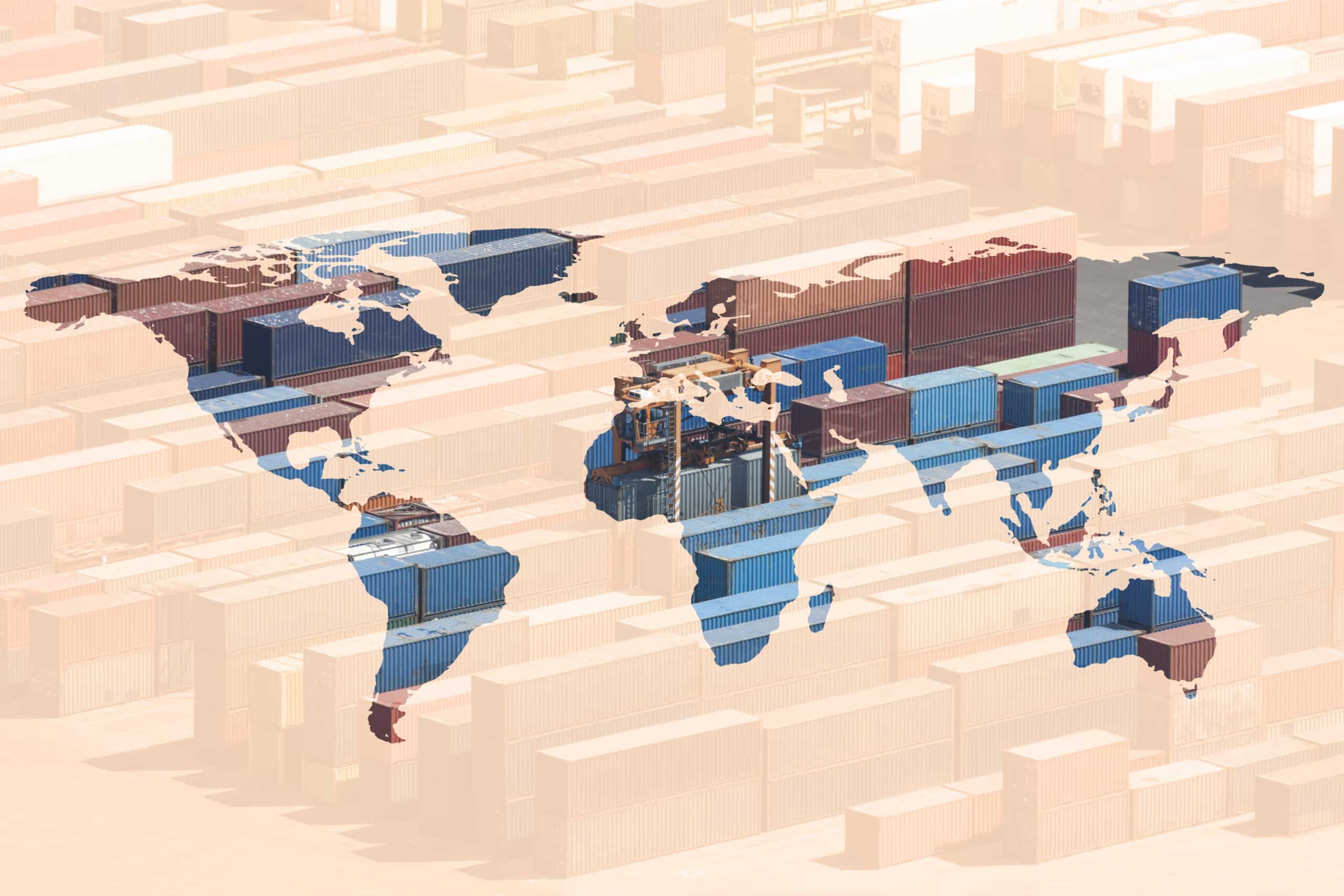
World map overlay on containers, symbolizing global trade and semiconductor supply chain resilience.

Semiconductor Supply Chain Resilience

One of the first questions the operating committee addresses is whether the BOM second-source list can absorb a forced substrate requalification without breaking the design-win pipeline. P&C Global's work on semiconductor supply chain resilience sits inside that decision and pairs tier-N visibility with the dual-use license inventory the trade-compliance lead already carries. S&OP cadence and the second-source posture close out the same engagement, so the design-win pipeline holds when advanced-node foundry allocation tightens.
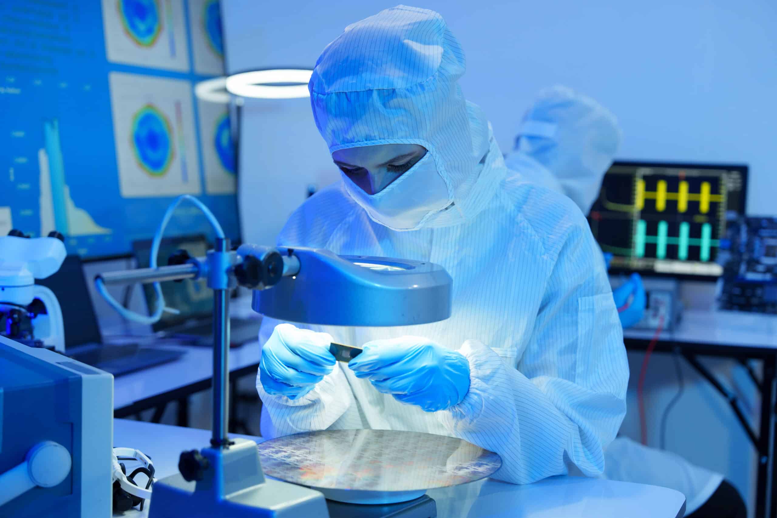
Scientist in cleanroom suit examines wafer under microscope during manufacturing operations consulting.

Manufacturing Operations

Yield performance through the node transition is now a board-level financial issue. P&C Global's semiconductor consultants work alongside the operating committee on manufacturing operations that hold OEE through the ramp and requalify tooling without disrupting qualified production revenue. The engagement lands with a yield-learning ramp the design review owns by cadence, not a benchmarking deck pulled together at the readout.

Product Management

Portfolio decisions for the chip business sit at the design review where the CTO and CFO already meet. The question on the table is which SKUs to ramp and which to retire single-source dependencies. P&C Global runs product management inside that meeting and maps the SKU portfolio against the design-win pipeline, so the operating committee can retire a node without leaving qualified revenue on the floor. The closing artifact is a portfolio decision log the board reviews against the next CapEx tranche.

Woman smiling and holding folders, standing indoors—perfect for growth strategy consulting firms.

Growth Strategy

Design-win conversion is where the growth thesis for a semiconductor business gets graded inside the operating committee. P&C Global runs growth strategy so the chief revenue officer and CTO can defend qualified-revenue ramp against allocation costs that exceed original planning assumptions. The engagement closes with a design-win pipeline the CFO actually believes, paired with the CapEx tranche release memo that funds the next node. What ships is the funded design-win plan, not another market-sizing exercise disconnected from execution realities.

Tall modern glass skyscrapers, an old church tower—urban growth meets capital investment strategy.

Capital Investment Strategy

Fab investment and packaging-line expansion both ride the same CapEx tranche the CFO defends to the board this cycle. P&C Global's semiconductor consultancy runs capital investment strategy so the next node decision lands with a tranche release memo the CapEx council can sign in writing. The payback model is rebuilt against current bill-of-materials realities, not carried forward from a model that already drifted. The engagement closes with a CapEx vs OpEx mix the board grades by hurdle rate, paired with the second-source list that protects the gross margin baseline.

Man in glasses presenting procurement strategy consulting data with bar and pie charts.

Procurement Strategy

Sourcing posture sits squarely on the operating committee's agenda when dual-use licensing reach keeps moving on substrates and tools. P&C Global runs procurement strategy so the chief procurement officer and CFO can hold a BOM second-source list the design review actually qualifies, not a vendor scorecard that has to be revisited every planning cycle. Engagements close with a sourcing posture the operating committee defends through the next node ramp, paired with an audit-ready dual-use license inventory.

R&D Consulting

Engineering capacity and design-tool throughput sit on the CapEx tranche right next to the fab build itself. P&C Global's semiconductor consulting services run R&D consulting so the CTO can defend engineering allocation against a tighter hurdle rate. The design review owns the trade-off between node investment and packaging build-out. The closing artifact is an R&D portfolio map the board reviews against the design-win pipeline, not a feasibility assessment that loses relevance when the node roadmap changes.

M&A Strategy

Consolidation in the chip industry has restarted, and operators are being asked to defend the next move against allocation pressure and dual-use licensing reach. P&C Global runs M&A strategy for the CTO and CFO who need to model a target's fab portfolio and trade-compliance posture against the acquirer's CapEx council. Engagements close with a deal thesis the board signs against the design-win pipeline, not a synergy model that loses operational relevance after close.

Technology Due Diligence

Pre-LOI diligence on a semiconductor target turns on whether the node and the substrate survive the acquirer's hurdle rate without forcing a costly substrate requalification later. P&C Global runs technology due diligence so the deal team can grade IP exposure and dual-use licensing reach before valuation assumptions are finalized. The CapEx tranche release memo gets modeled against the design-win pipeline the target actually defends. Diligence closes with a node-by-node payback view the audit committee meeting reviews, not a generic technology assessment disconnected from operating economics.


Outcomes Clients Can Expect

  • Lower unit cost per qualified wafer and a defended gross margin held through the node transition.
  • Stronger design-win conversion stability and a qualified-revenue ramp that does not retreat when foundry allocation tightens on advanced nodes.
  • Stronger engineering and supply-chain bench depth, with yield-learning expertise through the capital cycle.
  • Faster requalification on second-source substrate and tooling, supported by an S&OP cadence the operating committee formally governs.
  • Reduced single-source concentration and a defensible trade-compliance posture across wafer and dual-use flows.

Why Semiconductor Consultants Matter Now

The current semiconductor cycle is being evaluated against two operating realities at once. A trade-policy posture has to be defended on the dual-use license inventory the trade-compliance lead carries. A capital plan has to hold against a tighter hurdle rate the CFO defends to the board this cycle. That is now the environment semiconductor consultants are expected to navigate through the node transition. Foundry allocation no longer clears at the price the bill of materials carried last cycle. The design-win pipeline now depends on a second-source posture the operating committee defends in writing, not a vendor scorecard revisited every cycle under pressure. P&C Global runs the work end to end inside that scoreboard, pairing the design-win pipeline with the CapEx tranche release memo the board signs without reopening the investment case.

Strengthen Semiconductors with P&C Global

P&C Global’s semiconductor consulting embeds directly into the CapEx council and design-review cadence the operating committee already runs. The next node decision sits there, and P&C Global engages alongside the CTO and CFO to scope the work against the existing capital cadence.

Frequently Asked Questions — Semiconductor Advisory

Success Stories

A dynamic showcase of P&C Global’s transformative engagements and the latest industry trends.

Demonstrated Outcomes. Significant Influence.

Witness the remarkable achievements we’ve enabled for ambitious clients.

Harrods white

Luxury Retail as a Trusted Style Advisor

Client Outcomes Listing
Further Reading
target white

Winning the War for Technical Talent in Retail Product Management

Client Outcomes Listing
Further Reading
Digital Solutions that Empower Corporate Customers

Optimizing Corporate Card Management with Real-Time Innovation

Client Outcomes Listing
Further Reading
Private Equity Consulting

Elevating Talent Acquisition for Workforce Excellence

Client Outcomes Listing
Further Reading

Our Insights

Research & Insights
AI Agents & Autonomous Workflows: Redesigning Enterprise Execution
Further Reading
Research & Insights
Why Global 1000 Leaders Must Govern AI at the Enterprise Level
Further Reading
Research & Insights
Critical Lessons Learned to Combat the New Wave of Payment Fraud
Further Reading
By using this website, you agree to the use of cookies as described in our Privacy Policy